Precision Laser Marking for Electronics and Semiconductors
I once picked up a microchip from a failed circuit board and examined it under a loupe. The serial number etched onto its tiny 4mm × 4mm surface was flawless — perfectly spaced, crisp edges, and no visible heat damage to the surrounding material. That mark had been created by a UV laser in under 50 milliseconds. The chip itself had travelled from a fabrication plant in Asia, through PCB assembly, into distribution, and eventually onto a repair bench here in the UK — and that tiny mark made every step traceable. I put the chip down and started researching UV laser systems that same afternoon.

That moment captures why laser marking has become the standard across electronics manufacturing. From semiconductor packaging to PCB assembly and finished devices, manufacturers have steadily moved away from ink printing, adhesive labels, and other traditional marking methods. The reason is straightforward: only laser marks can survive the full production lifecycle that electronics must endure — soldering, cleaning, flux exposure, humidity testing, and years of real-world operation.
|
TRADITIONAL METHOD |
FAILURE MODE IN ELECTRONICS |
LASER SOLUTION |
|
Ink pad printing |
Smears in solder flux, fades in heat |
Laser marks are permanent — survive soldering, cleaning, flux |
|
Adhesive labels |
Peels in cleaning baths, trapped under conformal coating |
Direct part mark — no adhesive, no peeling risk |
|
Mechanical stamping |
Mechanical stress — cracks ceramic/polymer substrates |
Non-contact — no mechanical force on component |
|
Silk screen printing |
Requires drying time, ink contamination risk |
Laser marks instantly — no cure time, no chemicals |
|
Chemical etching |
Cannot achieve microscale precision required for ICs |
Laser spot sizes under 10µm for micromarking |
Electronics manufacturing presents a unique combination of challenges. Components are extremely small, often measured in millimetres or less, and materials vary widely from delicate polymers and ceramics to plated metals and silicon. At the same time, these materials are highly sensitive to heat, meaning even a slight excess of thermal input during marking can cause damage. Add to that the increasing demand for full traceability — from individual chips to finished products — and it becomes clear why conventional marking methods struggle to keep up. Ink can smear during soldering, labels can peel during cleaning, and mechanical methods risk damaging fragile components. Laser marking avoids all of these issues by providing a permanent, non-contact solution.

The real-world impact of this shift is significant. One UK-based contract electronics manufacturer, for example, replaced inkjet date coding with a UV laser marking system positioned before their reflow process. Previously, a noticeable percentage of their boards failed inspection because markings became unreadable after soldering and cleaning. Once they switched to laser marking, those failures effectively disappeared. The marks remained clear, consistent, and fully legible throughout the entire process. For their quality team, it was one of the simplest changes with the most immediate results.

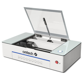
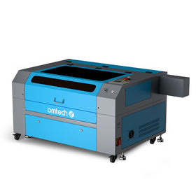
Different types of lasers are used depending on the material and application. UV lasers are the preferred choice for heat-sensitive components such as IC packages, PCBs, ceramics, and silicon wafers. Because they operate through a photochemical process rather than thermal ablation, they generate minimal heat, making them ideal for delicate materials. Fibre lasers, on the other hand, are used for metal components such as aluminium housings, stainless steel enclosures, connectors, and heat sinks. They produce high-contrast, durable marks at speeds that match production-line requirements. For more specialised applications involving plated materials, MOPA fibre lasers provide additional control over pulse duration, allowing precise marking without damaging thin layers of gold or nickel.

Across the electronics industry, laser marking is applied to a wide range of components. Printed circuit boards require serial numbers, batch codes, and compliance markings that must survive reflow soldering temperatures of over 260 degrees Celsius, as well as cleaning and coating processes. UV laser marks on these materials remain intact and readable throughout. Semiconductor packages and ICs present even greater challenges due to their small size, often requiring markings on surfaces just a few millimetres across. In these cases, UV lasers deliver high-contrast results without damaging the encapsulation, while MOPA systems handle plated variants safely.

As components continue to shrink, the importance of micromarking becomes even more apparent. Surface mount devices, such as resistors and capacitors, now have marking areas measured in fractions of a millimetre. UV lasers are capable of producing spot sizes under 10 microns, making it possible to create readable codes on surfaces that would be impossible to mark using traditional techniques. Similarly, connector terminals and lead frames often require selective removal of plating for both functional and identification purposes. MOPA lasers allow manufacturers to remove microns-thick plating layers with precision, eliminating the need for chemical etching or masking processes.
One of the most critical factors in all of these applications is thermal management. Unlike larger industrial parts, electronic components cannot tolerate excess heat. Even minor increases in temperature during marking can lead to cracking, delamination, or electrical failure. This is where UV lasers offer a significant advantage, as they break molecular bonds directly rather than heating the material. The result is an extremely small heat-affected zone, ensuring that surrounding areas remain unaffected. MOPA systems address similar challenges in metal and plated components by allowing precise control over energy delivery, reducing heat spread and protecting the underlying material.
In modern UK manufacturing environments, laser marking systems are often integrated directly into production workflows. They connect with ERP and MES systems to enable real-time serialisation and batch tracking, ensuring full traceability across the supply chain. This is particularly important for compliance, as products destined for UK and European markets must meet strict marking requirements. These typically include UKCA marking for domestic compliance, CE marking for EU distribution, and adherence to RoHS regulations. Laser marking ensures that these identifiers remain permanent and legible throughout the product’s lifecycle.
The information marked on electronic components varies depending on the application but generally includes manufacturer logos, date codes, batch numbers, serial numbers, and increasingly, 2D Data Matrix codes. These codes are especially valuable because they can store large amounts of data in a very small space, making them ideal for compact components. Their durability and readability are essential for maintaining traceability in complex supply chains.
For many UK manufacturers, adopting laser marking is not simply a technical upgrade but a strategic decision. It eliminates the need for consumables, reduces the risk of quality failures, and improves production efficiency. Perhaps most importantly, it ensures that traceability requirements are consistently met without adding complexity to the process. In an industry where reliability and compliance are critical, laser marking has proven to be one of the most effective and practical solutions available.