Top 5 Laser Engraver Applications for Electronic Chips
The first, and most important thing to know about laser processing semiconductor packages is that it is highly specialized. A single mistake can destroy the chip, compromise performance, violate compliance standards, or even create legal and ethical problems for your company.
So, before buying a laser engraving machine or beginning an electronic chip engraving project, it is important to thoroughly understand the demands and requirements of the project, the nature of the material being processed, and the right type of laser system for the task.

Top 5 Key Applications of Laser Engraving on Electronic Chips
1. Part Marking and Traceability Codes
Part marking and traceability codes are two of the most common and legitimate uses of lasers on electronic chips, and it is mostly done by manufacturers who need to mark serial numbers, lot codes, QR codes, logos, and date codes on materials like integrated circuits, chip packages, and boards.
If you are a semiconductor manufacturer, an electronics assembly plant, an automotive electronics supplier, or a medical electronics manufacturer, this is most likely the primary reason you need a laser engraver.
2. Surface Coating Removal
Repair technicians, electronic refurbishers, rework labs, and quality control teams deal with chips and components that have coatings, epoxies, paints, or conformal layers that need to be selectively removed.
With UV lasers or low-power CO2 lasers ( depending on coating composition), they can remove thin coatings with precision while minimizing contact damage. This is useful when you need to expose pads, labels, or hidden surfaces.
Usually, this includes using high-powered lasers (like 10W to 20W fiber lasers) to ablate the black epoxy casing off chips to reveal the raw silicon die underneath.
Surface coating removal is another key application of laser engraving on electronic chips, and it is most common for companies or businesses dealing with the repair or refurbishment of old electronic appliances.
3. Failure Analysis Preparation
Using laser engraving for failure analysis preparation is especially common in reliability labs, semiconductor testing facilities, R&D departments, and engineering failure analysis teams.
These companies sometimes need to expose certain package areas or prepare a component for microscopic inspection during troubleshooting.
So, they use UV laser engravers to carry out controlled material removal with very small heat-affected zones.
Laser engraving is great for this application specifically because it not only gets the job done but also helps preserve the surrounding structures.
4. Package Trimming or Micro Modification
Prototype labs, specialized manufacturers, and advanced engineering teams use laser engraving for package trimming and making micro modifications.
Though this is not the most pivotal laser engraving application in the electronic chip industry, it is important for these institutions that require trimming package materials, resizing molded housings, or creating openings for engineering access.
With the high precision and repeatability of a fiber laser, they are best able to handle these jobs that often involve expensive components, where scrap costs are high.
5. Anti-Counterfeit and Security Marking
Some manufacturers, such as OEM brands, high-value electronics manufacturers, and defense contractors, use hidden or micro-scale marks to authenticate genuine components. This is often called “blacktopping”, where companies use lasers to wipe serial numbers off chips to protect intellectual property.
With a UV laser or high-resolution fiber laser, they are able to create marks that are difficult to replicate and easy to verify under magnification.
Overview of Applications of Laser Engraving Electronic Chips
Broadly speaking, there are two ways laser engravers are used on electronic chips: some professionals use them for legitimate identification marking, traceability, failure analysis, package modification, or selective material removal. These are the more conventional uses, and what you will most likely see out there.
Other users, however, use laser engravers for more “controversial” uses, like decapsulating chips for inspection or obscuring part numbers to reduce reverse engineering risks.

Best Laser Engravers for Electronic Chip Engraving
Electronic chip engraving is done exclusively with fiber lasers and UV lasers. Fiber lasers are the gold standard for electronic engraving applications, but UV lasers are highly recommended because they are also capable of making clean markings without damaging internal components.
Diode and CO2 lasers are generally ineffective and can even be dangerous for electronic chips: they can melt the epoxy or release toxic/corrosive smoke, resulting in tons of safety issues and costly damage to the material.
1. Fiber Laser Engravers for Electronic Chip Engraving
Fiber laser engravers are best for electronic engraving, principally because they generally use a 1064nm. This higher wavelength makes a big difference in electronic chip engraving because it efficiently marks or vaporizes the plastic/epoxy resin used in IC packaging without creating massive heat-affected zones. As a result, fiber laser engravers are fast, reliable, and excellent for permanent industrial marks.

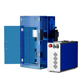
Equipped with a Galvo Laser Drive and optical lenses, OMTech Galvo Fiber laser machines are optimized for use in high-volume factories, metal package processors, and rugged industrial production lines. With models ranging from 20W to 100W, they can handle demanding electronic chip engraving projects like metal shields, metal lids, durable ID marks, and security marks.
2. UV Laser Engravers
UV lasers are often the preferred option for delicate electronics work, especially for chip package marking, QR codes, fine logos, and coating removal. The advantage of UV laser engravers is that they are great for clean markings and safe to use for electronic chips.
3. CO2 Laser Engravers
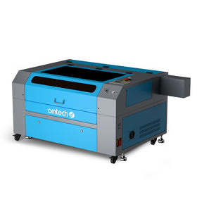
CO2 laser engraving machines are generally not used for direct chip work, but they can be extremely useful for related tasks like burning temporary paint masks when etching custom PCBs. CO2 laser engravers are used by electronic chip facilities that also work with processing trays, packaging, labels, or non-chip plastics, and mixed-material production shops.
OMTech’s Pronto CO2 Laser engravers offer the appropriate mix of versatility, dependability, and safety that is needed in an electronic chips processing environment.
With a top engraving speed of 1000mm/s (37% faster than competitors) and an upgraded transmission system for superior accuracy in every detail, they are fast, safe, and reliable. The Pronto’s maximum workpiece height is 8.7 inches, an impressive 83% increase that accommodates taller items.
In short, CO2 lasers excel with many non-metallic organic materials, though they are usually not the first choice for fine semiconductor package marking.
Recommended Laser Engravers for Electronic Chips
| Laser Engraver Type | Wavelength | Common Electronic Chip or Related Applications | Recommended Laser Engraver | Key Notes |
| Fiber Laser Engravers | 1,064nm | Metal shields, metal lids, durable ID marks, security marks | OMTech Galvo Laser Engraver Series | Excellent for demanding production environments and permanent marking on metals |
| UV Lasers | 355nm | Chip package marking, QR codes, fine logos, coating removal | Cloudray UV Laser Engraver | Best for delicate materials, high precision, and low heat impact |
| CO2 Laser Engravers | 10,600nm | Packaging labels, trays, plastic housings, and non-chip surfaces | OMTech Pronto 60W CO2 Laser Engraving Machines | Less common for direct chip work, but useful for surrounding materials and accessories |
Critical Tips and Warnings When Laser Engraving Electronic Chips
- Heat damage is the biggest risk. Excessive energy from a laser engraver can crack packages, damage bond wires, alter internal structures, or destroy functionality. Always start with test samples and conservative settings.
- Know the package material. Chip packages may be epoxy, ceramic, metal, resin, or composite materials. Different materials react differently to laser wavelengths and power levels.
- Ventilation is essential. Lasering polymers, resins, or coatings can release fumes and particulates. Use proper extraction and filtration systems.
- Mark only the non-critical areas. Never engrave blindly on active surfaces, thin walls, leads, or areas near sensitive structures.
- Verify legal and ethical Use. Altering part numbers, removing identification, or processing chips without authorization may create compliance, warranty, or legal issues. Always confirm ownership, regulatory requirements, and permitted use.
- Use microscopic inspection. Chip-scale work often requires magnification before and after processing. Small defects may be invisible to the naked eye.
 Final Thoughts on Laser Engravers for Electronic Chips
Laser engravers can be incredibly useful tools for electronic chip applications when used correctly. They support traceability, security marking, inspection prep, and specialized package processing. However, chips are not ordinary materials. They are small, heat-sensitive, and costly, which means the wrong laser or poor settings can cause immediate damage.
For most delicate semiconductor marking tasks, UV lasers are often the safest and most practical choice. Fiber lasers shine in industrial marking environments, while ultrafast systems dominate advanced microprocessing. The best machine depends entirely on whether your goal is identification, inspection, package modification, or production efficiency.
For more valuable information, explore our complete guide on precision marking for electronics and semiconductors.